![]()
![]()
![]()
Level 1
Section 5.4: Introduction to laser machining of semiconductors
The major semiconducting materials are the covalently bonded elements silicon and germanium as well as a series of covalently bonded compounds including GaAs, CdTe and InP, among others. In some ways semiconductors are a subclass of ceramics, since their bonding characteristics and mechanical properties are similar to those previously described for ceramics. The commercial importance of semiconductors, however, warrants their consideration separately. For these materials to exhibit the level of reproducibility of properties required by the microelectronics industry, semiconductors must be processed in ways that permit precise control of composition and structure. In fact, the processing techniques for semiconductors are among the most highly developed of those used for any materials class. For example, impurity levels are routinely controlled in the parts-per-billion range (i.e., a few impurity atoms for every billion host atoms). The previous discussion on composites focused on materials used for structural applications. It should be understood that microelectronic devices are essentially composites in which a host of radically different property requirements means that different classes of materials (metallic conductors, active semiconducting elements, and ceramic insulators) must be used in close proximity. One of the major challenges in the area of microelectronics lies in miniaturization and fabrication of these devices. The extremely fine scale of current microelectronic devices is shown in Figure 1.
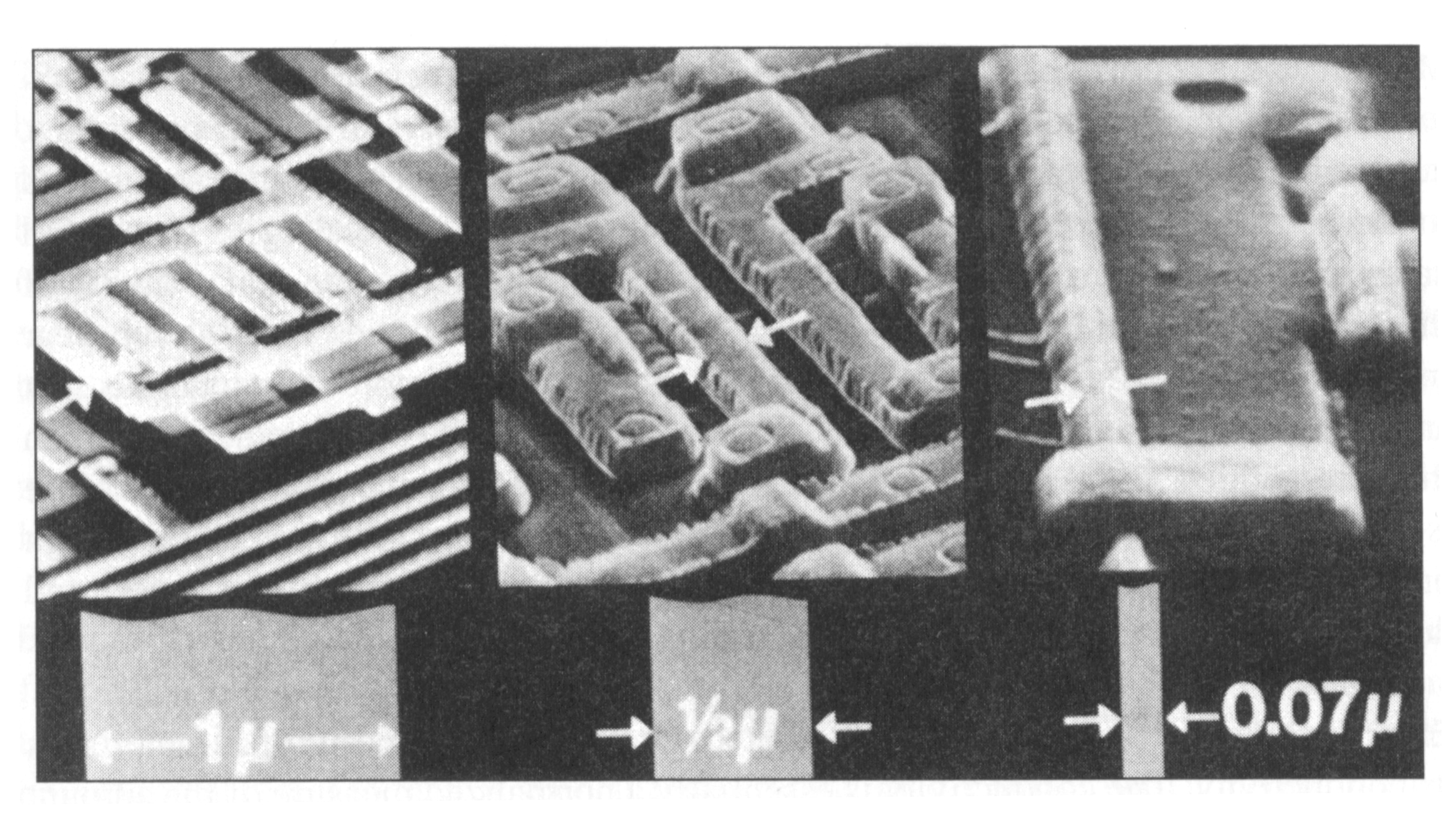
Fig. 1 Microelectronic circuits. Note the very small size of the features on these devices (Courtesy of the National Academy Press, Washington, D.C.)
Here it is clear that many of the components of this composite structure are of submicron size! Some current and potential applications for semiconductors and microelectronic devices are listed below:
- The dominant mode of information transfer is changing from electrical to optical signals. While the technology for optical communication has already been developed, the materials and devices for optical computing are still in the research stage. It is believed, however, that the developing technology will result in much faster and therefore more powerful computational devices.
- Over the past few decades the size of these devices has decreased to the extent that it is now possible to place several million of them in an area of less than 1cm2. The size scale of microelectronic devices continues to decrease. While a typical "chip" in a 486-computer contains about 1 million devices, by the year 2000, "chips" contains on the order of 100 million devices. This results in smaller, faster, more powerful electronic devices of all kinds.
- Micromachining is a relatively new technology in which mechanical components, such as miniature motors, are incorporated directly into the silicon chip. In this way the electrical and mechanical components are intimately linked in a manner that leads to decreased size as well as increased reliability and device performance. An example of this technology is the device used to trigger air bags in many automobiles. The mechanical component (an accelerometer) recognizes the rapid deceleration and initiates an electrical signal that results in the deployment of the air bag. The prefix micro in microelectronics reflects the fact that a typical device dimension is now on the order of a micron or less. Examples of microelectronic devices include the pn junction diode and npn bipolar junction transistor described in the previous section. These and other devices can be linked together to fabricate microelectronic circuits, known as integrated circuits (ICs), ranging in complexity from a simple amplifier to a complete miniature digital computer known as a microprocessor. Many of the key issues in the microelectronics industry are related to the materials, properties, and processing of semiconductors.
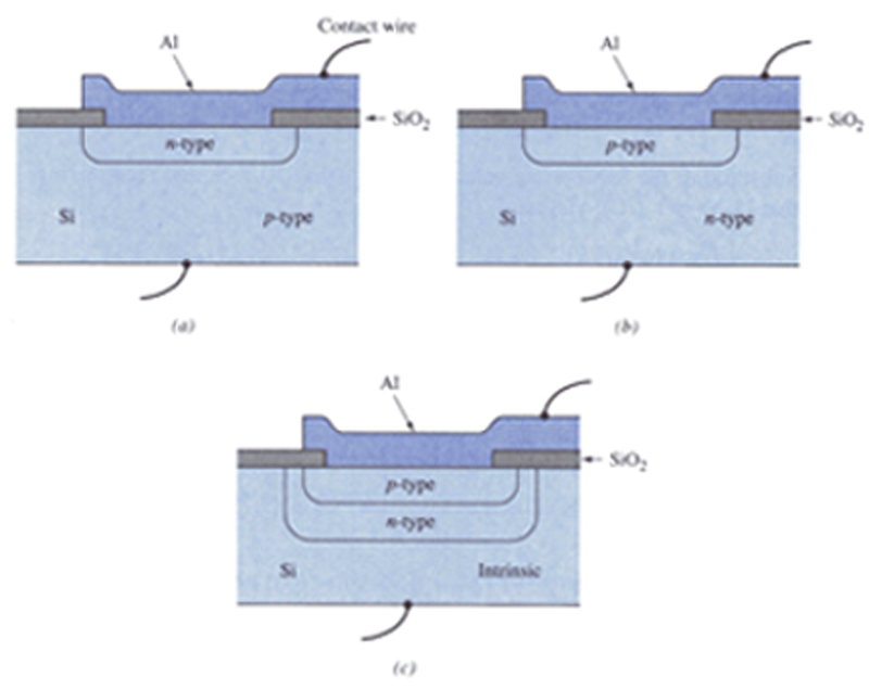
The first semiconducting devices were fabricated from Ge. It was soon realized, however, that Si offered several advantages, including its lower raw material cost, its larger band gap, which permits operation at higher temperatures, and the superior characteristics of its natural surface oxide, SiO2. To understand the significance of the oxide layer we must describe some of the processing operations used to fabricate integrated circuits. From a materials point of view an IC is a thin piece of intrinsic semiconductor, often Si, with well-defined surface regions processed to contain known amounts of electrically active dopants. Figure 2. shows three methods for fabricating a pn junction diode: (1) a controlled amount of an n-type dopant can be diffused into a p-type substrate, (2) a p-type dopant can be diffused into an n-type substrate, or (3) if the substrate is intrinsic, two sequential diffusion operations are required. One of the key steps in the process is the definition of the spatial region over which the dopant is introduced.
Fig. 2 The method for fabricating a pn junction diode: (a) diffusion of an n-type dopant into a p-type substrate ; (b) diffusion of p-type dopant into n-type and p-type dopants into an intrinsic substrate. (After James P. Shaffer, et al., 1995)
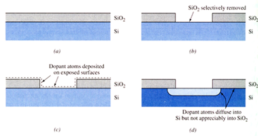
As shown in Figure 3, this is accomplished by selectively removing the SiO2 surface layer above the region to be doped. The dopant is then introduced onto the surface and thermally diffused into the substrate. Since the rate of diffusion is substantially slower through the SiO2 than through the Si, the shape of the window in the oxide effectively defines the shape of the doped region. In addition, SiO2 is a high-quality electrical insulator that can become an integral part of an active device.
Fig. 3 The method for introducing a controlled amoiunt of a dopant into a silicon substrate: (a) the SiO2 surface oxide layer is removed from the region to be doped. (b) dopant atoms are introduced onto the surface and (c) the dopant is thermally diffused into the underlying silicon. (After James P. Shaffer, et al., 1995)
For example, consider the metal-oxide-semiconductor (MOS) capacitor shown in Figure 4. As described in detail in the next chapter, a capacitor is formed by placing a thin layer of insulating material, in this case SiO2, between two conducting layers.
Fig. 4 A metal-oxide-semiconductor (MOS) capacitor. (After James P. Shaffer, et al., 1995)
This useful electrical characteristic of SiO2 coupled with its ability to block diffusion of many types of dopants are two key factors promoting Si as the material of choice in most microelectronic applications. Not all ICs, however, are fabricated from Si. For example, the speed of a device is limited by charge carrier mobility. The electron mobility in GaAs is more than 4.5 times higher than in Si. Thus, GaAs is one of the materials of choice in high-speed and high-frequency (GHz) applications. Another interesting semiconducting material is SiC, which offers several advantages over Si, including superior resistance to chemical attack and improved high-temperature stability. As such, SiC is often preferred for use in aggressive environments. SiC can be doped either n- or p-type; however, its principal disadvantage is that it is difficult to grow high-quality inexpensive single crystals. The polymer-based and organic semiconductors are relatively new materials and are not yet fully understood. They have the potential to become extremely important, especially in biological applications. In addition, it is likely that their low mass density, anisotropy, and good ductility will be harnessed to create new classes of semiconducting devices. Since these semiconductors have low charge carrier densities and mobilities, their properties are extremely sensitive to the presence of impurities.
Laser irradiation can change the semiconductor material's microstructure during the varied rapid heating (melting) and cooling (solidification) scenarios in which far from equilibrium conditions prevail. In particular, the process has been shown to involve heat flow and phase transformations. Therefore, semiconductor material's mechanical and electronic/optic properties are can be manipulated in many modern technologies.
Pulsed excimer-laser processing of amorphous silicon on non-crystalline substrate is an important processing technology for large-area polysilicon electronics, such as flat-panel displays and two-dimensional imaging arrays. It also allows for the integration of amorphous silicon and polysilicon devices on the same glass substrate and provides procedures for the doping of self-aligned thin-film transistors. Materials studies show that laser-crystallized polysilicon exhibits a narrow peak in the average grain size as a function of the excimer laser energy density, with a corresponding peak in the electron mobility. This is of particular significance for devices since large grains imply high electron mobility. On the other hand, the peak in the grain size is very narrow and is also accompanied by a peak in the surface roughness of the film. These relationships force a compromise between large grain size for high mobility and homogeneous size distribution for uniformity of device characteristics. Laser-processing enhancements, such as laser doping and fabrication of self-aligned transistors, provide additional tools to fabricate unique devices.
The electrical characteristics of excimer laser annealed (ELA) polycrystalline-Si thin film transistors (poly-Si TFT's) were investigated by (Kubo, Nobuo, et. al., 1994). These results were compared to those of poly-Si TFT fabricated by solid phase crystallization (SPC). From the temperature dependence if the drain current, the activation energies of n-type poly-Si TFT's were obtained. The activation energies have negative values under the gate voltage from 0 to 5 V. The negative activation energy together with small threshold voltage (Vth) are the main characteristics of ELA poly-Si TFT. From these results, it is concluded that the trap state density of ELA poly-Si TFT is very small and the electrical characteristics can be explained by the band tail states localized at the grain boundary.
Semiconductor oxide recrystallizes under laser irradiation. Kinetic regularities in sintering polycrystalline metal oxides are studied at the stage of diffusion grain growth under laser exposure (Alimoy, D.T 1991). It is shown that the rate of mass-transfer between separate grains changes as a function of frequency characteristics and exposure intensity. For experimental support of the assumption that the distribution function deformation under laser exposure results from variations in the grain growth-grain size relationship the grain growth kinetics is measured. Mechanisms are offered to connect grain growth rate and electronic crystal subsystem disturbance.
Laser induces the formation of titanium silicides. Chen. X.Y (1999) reported on the laser-induced formation of both C49 and C54 TiSi2 films with fine grains using Q-switched Nd:YAG laser irradiation from Ti/Si samples. The films formed were characterized with micro-Raman spectroscopy, high-resolution transmission electron microscopy, energy-dispersive spectrometry and atomic force microscopy. The TiSi2 films synthesized are single-phased and thin, with fine grains and a smooth film/substrate interface on the atomic scale. The process is likely to proceed via a solid-state reaction rather than liquid-phase intermixing. Our results demonstrate the unique advantages of a laser annealing technique and its potential in deep submicron semiconductor technology.
Laser processing is widely used for fabrication of electronic components. Applications include trimming of resistors, hole drilling, scribing, and marking. Lasers may also be used to fabricate microcircuit via the controlled deposition of semi- conductors, metals, and insulators. We will emphasize currently used applications in electronic fabrication. Many of these applications involve material removal, in applications such as substrate drilling and cutting. We will also discuss developing approaches to use of lasers in integrated circuit fabrication. A variety of different types of lasers are used in electronic fabrication. The use of the CO2 and the infrared ND:YAG lasers in electronic processing applications is well established; these lasers have been used for many years for applications such as trimming and drilling. The green and ultraviolet lasers may be focused to a smaller spot than the infrared devices, and they may be chosen when small focal diameter is desired. The use of ultraviolet lasers is relatively new, especially the excimer and frequency-tripled and -quadrupled ND:YAG lasers. These lasers have become more mature and reliable, and they now present viable options for electronic processing. They offer the attractive feature of very high absorption in many materials of interest. Lasers have reached production status for a variety of applications in the electronics industry. One of the most significant is the trimming of resistors. This can significantly increase the yield in the processing of resistive elements. Resistors for use in electronic circuits may be printed on a substrate from a liquid ink and subsequently fired and dried. Such resistive elements are called thick film resistors. In some cases, resistors are formed by vacuum deposition of metals. These resistive elements are called thin film resistors.
Established Applications in Electronics
In either case, it is difficult to control the value of the resistance to within the tolerances required by the circuit. Thus, resistors are fabricated with intentionally low values of resistance and then trimmed by removing material from the conducting path. The value of the resistance may be monitored during the trimming process, and the trimming is terminated when the desired resistance, is reached. Alternatively, the performance of the circuit may be measured during trimming; in this case, the trimming is terminated when the circuit is operating properly.
Trimming by laser ablation of material from the resistors has become wide spread. The technique most often uses a repetitively Q-switched ND:YAG laser, emitting a train of pulses with peak power in the kilowatt range, pulse durations around 250 nsec, and pulse repetition rates in the kilohertz regime. The ND:YAG laser offers the advantage of smaller cut widths than the carbon dioxide laser, which has also been used. The infrared ND:YAG laser is perhaps the most common choice, but if fine trimming cuts are desired, the frequency-doubled ND:YAG laser is employed. Trimming with excimer lasers has also been demonstrated, but this has not yet become common. Various geometries for cutting have been used. A popular geometry is the L-shaped cut. The resistor is cut partway across, and then the direction of travel is changed by 90 degree. This leads to finer control of the process. If one simply continued to cut straight across the resistor, there would be relatively poor control of the tolerance when the cut reached almost all the way across the resistor. The percentage change in resistance per unit cut length would become very large. The L-shaped cut allows a more gradual approach to the final desired value.
Thermal shock and damage along the cut, which cause drift of the resistor after trimming, have been problems. Keeping the laser power down to the minimum needed for a clean cut will reduce problems of damage and post-trim drift. With careful control, the change in resistance after the trimming can be in the range around 0.1 percent or less. Laser trimming of resistors is especially notable because it is a process that has become routine in the electronics industry, and it has essentially replaced the older method, which was abrasive trimming. Laser trimming offers the advantages of better cleanliness and better control over the final resistance. The laser trimming operation results in a higher yield; that is, a larger fraction of the resistors are within the prescribed tolerance.
Laser-based removal of material from substrate is also widely used for shaping, drilling, and cutting of substrate. Pulsed carbon dioxide lasers are commonly used to drill holes in alumina substrates for circuit boards. Alumina ceramics absorb well at the CO2 laser wave- length. Laser drilling in hard, high-temperature-fired alumina ceramic is attractive because drilling ceramics by conventional means is expensive. It usually requires diamond-tipped drill bits, which are subject to breakage. Conventional drilling of holes less than 0.25 mm in diameter is difficult. Laser drilling easily produces small holes in this brittle material without danger of fracturing it. When a pulsed CO2 laser is used with alumina of thickness less than 1mm, typical hole diameters may be in the range of 0.1 to 0.2 mm with tolerances around 0.02 mm. Because of the brittleness of these ceramics, conventional hole drilling is usually performed on the material before it is fired. When it is fired, the dimensions may change. Laser chilling is performed after firing, thus eliminating this potential problem.
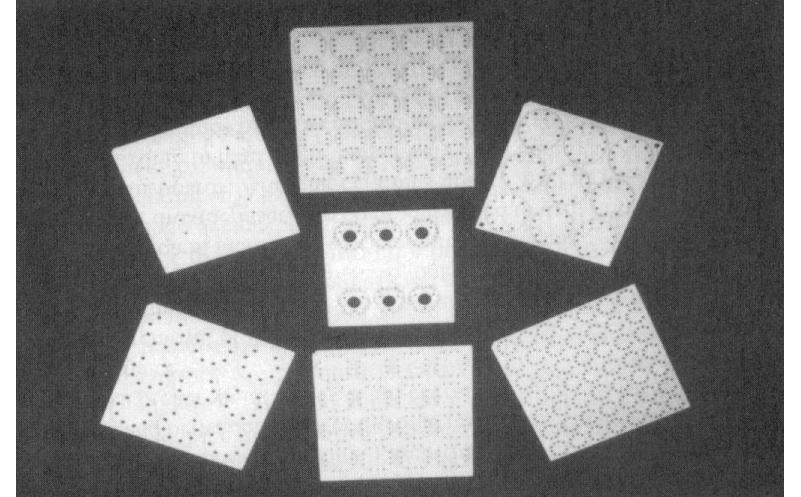
Automated laser systems drill complicated patterns of holes in material about 0.6 mm thick. The system includes fixturing to hold the ceramic, a stepping motor to move the fixture to predetermined positions at which the holes are to be drilled, and a control to turn the laser on and off so that holes are drilled in the prescribed positions. The entire process may be automated to yield as a final result the desired pat- tem of holes in the ceramic. Figure 5 shows examples of laser-drilled holes in alumina substrates. Lasers are also used to cut or shape a wide variety of nonmetallic substrate materials. Many cutting operations have employed carbon dioxide lasers because of their capability for producing high values of continuous power and because the CO2 laser radiation is absorbed well by ceramics. Cutting of nonmetallic materials, such as alumina or silicon, proceeds easily. A continuous CO2 laser operating at a level around 100 W is adequate for many cutting applications. The advantages of laser cutting include lack of tool wear, reduced loss of material around the cut, higher yield because of reduced breakage and rapid turnaround because of the ease of fixturing. An alternative to cutting of materials like ceramic is scribing. In scribing, a series of closely spaced or overlapping blind holes is drilled partway through the sample. The material will then easily snap along the path defined by the laser scribe line. Usually, scribing is done in a straight line in order to provide a clean separation, without random cracking, in the desired path. Scribing is widely used for applications like dicing alumina substrates into chip carriers or separating silicon wafers into chips. The scribing of alumina uses carbon dioxide lasers and the scribing of silicon is done with ND:YAG lasers, because the absorption of the different materials is high at the different wavelengths. The motivation for scribing rather than cutting is that the scribing rate is higher than the cut- ting rate. For alumina around 0.025 in. thick, the material may be scribed at rates around 10 in./sec with an intermediate-power CO2 laser, whereas cutting rates may be a few tenths of an inch per second for a similar laser. Scribing also offers the advantage that a substrate may be scribed before processing is completed and then easily separated into chips after processing.
Fig. 5 Examples of patterns of laser-drilled holes in Aluminia ceramics substrates.(Photograph courtesy of Electro Scientific Industries, Inc.)
There are many requirements for identification of manufactured parts in electronic fabrication. Product marking is carried out for purposes of identification or imprinting product information. Conventional techniques include printing and stamping. Laser marking provides an attractive alternative for durable permanent marks with no possibility of contamination. Two different laser-based approaches to marking of electronic products are employed. In the first method, one scans the focused high-power beam over the surface of the part and modulates it to vaporize a small amount of material at selected positions. The mark thus consists of a dot pattern. In the second method, called image micromachining, the pattern is formed all at once, by delivery of a high power beam already focused in the desired pattern. The first method is applicable to marking of materials that require relatively high energy to vaporize, for example, silicon wafers. The second method is applicable for softer materials that require lower energy per unit area, such as packaging materials. Laser printing of identifying numbers on silicon wafers is attractive because of the brittleness of the material, because subsequent manufacturing operations could destroy printed marks, and because marking with inks represents a potential source of contamination. ND:YAG lasers are generally used for this application because silicon absorbs well at wavelengths near 1 micron, whereas it does not have high absorption at the carbon dioxide laser wavelength.
Laser vaporization is also used to remove small amounts of unwanted metallization, for example, on master patterns used for making photographic masks for integrated circuit chips. This use, which has reached routine production status, is employed to reduce the number of defects per mask, and thereby to increase the yield of the process. One desires typically a short-wavelength laser, often a frequency-doubled ND:YAG laser operating at 532 nm. The absorptivity of the metal is relatively high at this wavelength. Because of the short wavelength, the beam may be focused to a very fine spot. The masks are subjected to visual inspection under a microscope with a display on a television monitor. The surface of the mask is scanned in a pattern. When a spot of undesired metallization is located, it is lined up in the center of the display with grid marks to indicate the aiming point. The diameter of the focused beam is adjusted to accommodate the size of the particular spot of metallization. The laser is then fired, delivering a pulse that vaporizes the unwanted metallization. In addition to drilling holes in substrate materials, laser ablation is used to fabricate vias for the fabrication of multichip modules and in printed wiring boards. The vias are then metallized in order to form an electrical contact from one side of the material to the other.
In the production of multichip modules, vias are formed in polyamide by excimer laser ablation. Excimer lasers have been used for this application because of the very high absorption of plastic materials in the ultraviolet portion of the spectrum. Typical laser parameters used have been 150-300 mJ/cm2 at 308 nm wavelength (XeCl excimer laser). Projection through a mask has allowed drilling of many holes at the same time on fields in excess of 100mm square. This technique has been used to fabricate many billions of 6-gm-diameter vertical interconnection vias. The laser drilling has proved to be faster and less expensive than the competing techniques of wet etching or reactive ion etching. Laser drilling has also been investigated for drilling printed wiring boards. In such boards, the density of conductors is limited by the presence of relatively large pads. Pad size is determined by the diameter of vias under the pads. Reduction of via and pad size is desired to increase component density. Current technology has used numerically controlled mechanical drillers. Costs have been high, and they increase rapidly as the via size decreases. The minimum practical via size is about 150 gm with mechanical drilling. Several laser types have been investigated for this application. Excimer lasers have excellent absorption in polymeric materials. They can produce very clean holes in the 6-60 gm diameter range. Removal rates are low, so that costs are high except in fixed designs with mask imaging where many vias can be drilled simultaneously. This application has reached limited production.
Frequency-tripled and -quadrupled ND:YAG lasers can drill vias with diameter in the 25-50 gm range. Drilling rates are faster and costs lower than for excimer lasers, but more precise control is needed. These lasers appear to be competitive for via drilling. Carbon dioxide lasers are also candidates for via drilling. The absorption is high al the CO. laser wavelength, and the drilling rate is high. The hole sizes are larger than for the shorter-wavelength lasers, but CO2 lasers appear econoniicoy competitive. Another application of laser ablation is the cutting of links in a circuit. In circuits like arrays of memory cells, one may insert extra columns or rows of elements in the array. The devices are tested, and faulty devices are identified. Then, the laser is used to vaporize the conductors that link the rows containing faulty elements. The faulty devices are thus removed from the circuit. This technique has been widely used to repair memory arrays. It provides redundancy for dynamic random access memory (DRAM) yield enhancement. It has also been used for personalization of multichip modules and for application specific integrated circuits (ASICs). Frequency-doubled ND:YAG lasers are frequently used for such repair and personalization. Lasers have also been used for link formation. Multilayer substrates with an incomplete top layer are fabricated. The top layer may be only bond pads. Lower layers are generic, design-independent wiring patterns. Spot links may be fabricated in a maskless deposition process. This procedure is useful for applications like customization through simple laser spot links, fast turnaround processing, fabrication of ASICS, and personalization of multichip modules.
Frequency-doubled ND: YAG lasers are also used in this application. One approach to laser link making has been to use materials like copper forrnate. A solution of copper formate in water is spun onto a wafer, and a solid film is dried from the solution. The film is decomposed in selected areas by a frequency-doubled ND:YAG laser to leave copper metallization, which forms the interconnecting links. The remaining film is then washed off with water. Other metal-organic compounds are also available if other types of metal interconnects are desired.
In another interconnection application, laser tape-automated bonding (TAB) of leads to integrated circuit input-output pads offers advantages compared with conventional techniques like thermocompression bonding. Because of its localized nature, laser bonding has less chance of damaging the chip. It has also provides stronger bonds. TAB has commonly been performed with millisecond pulse ND:YAG lasers. Materials that have been used include gold, copper, and tin. The rate of formation of the bonds can be high, greater than 60 per second. This application is still relatively small but appears to be growing.
Another application involving material removal is the stripping of insulation from wires, in preparation for making an electrical contact to the end of the wire. Laser ablation of the insulation on wires can be performed in a wide variety of cut patterns knd can remove hard or high-temperature insulation. It does not cause nicks, scratches, or broken wire strands, as mechanical removal of insulation sometimes foes. Laser stripping of wires has reached production status. It has most frequently been performed with CO2 lasers, but recent studies have indicated that excimer lasers can produce clean, well-defined cut patterns, with very little residue. For stripping of polyurethane insulation in particular, the use of excimer lasers can provide greater precision and cleanliness than CO2 lasers.
A final packaging application involves hermetic sealing of electronic packages by laser welding. This has become a common production application, especially for the sealing of microwave packages. Previously, tungsten-inert gas (TIG) welding and resistance welding were common, but these techniques produce large heat-affected zones and deliver relatively large amounts of heat to the package. The advantage of laser welding is the very localized heating involved, so that there is no damage or distortion of the delicate components in the package. The heat-affected zone associated with laser welding is smaller than for the competing techniques. Laser welding provides production package sealing with excellent hermeticity and good shock and vibration tolerance. One common material for microwave packages is 6061 aluminum. This alloy is somewhat brittle, so that use of a filler material is desirable to avoid cracking of the weld. Aluminum alloy 4047, containing about 12 percent silicon, has proved useful as a filler. Packages are often welded by an infrared ND:YAG laser with pulses in the millisecond regime. Typical welding conditions for aluminum packages might be an average power of a few hundred watts, pulse duration of a few milliseconds, and pulse repetition rates of a few tens of hertz. Seam rates might them be in the 50-100 in./min range. Hermetic sealing of packages in production by laser welding has become common practice, especially when components in the package are heat sensitive. The foregoing examples present only a few of the many practical applications of laser processing that have become established for fabrication of electronic structures and components.
Applications in Integrated Circuit Fabrication
Laser processing has been used in the electronics industry for many years for applications such as described in the previous section. The applications discussed to this point have involved components in an electronic assembly, such as resistors and substrates, packaging of the devices, and repair. We have not yet discussed applications involving fabrication of integrated circuits. Fabrication of integrated circuits has been performed by optical lithography for decades. In the photolithography process, photoresist is exposed through a mask that is imaged on the surface of the resist to produce the features of the microcircuit. Current sources for photolithography employ mercury lamps to a large extent. Feature size in integrated circuits has steadily decreased, and it will continue to decrease, with concomitant increase in chip density. Significant advances in optical lithography technology have been required to make this possible. The shrinking feature sizes in microelectronics require that lithographic sources move to shorter wavelengths, to the deep ultraviolet. Feature sizes in the mid 1990s are in the 0.35 /im regime. But conventional light sources (mercury lamps) cannot deliver enough en- ergy with the required resolution, as feature sizes continue to shrink, to the 0.25 gm region and below. In addition, the relatively broad linewidth of the mercury lines is a problem. There are very few optical materials suitable for use at wavelengths of 250 nm or less. These include fused quartz and a few fluoride materials (calcium fluoride, lithium fluoride, etc.). Only one material, fused quartz, is suitable for use in high-quality optical projection systems. With only one material available, one cannot design an optical system that incorporates color correction. Thus, the linewidth of the optical source must be very narrow.
The current mercury lamps, operating at a wavelength of 365 nm, should be adequate to support the production of 64 megabit dynamic random access memory (DRAM) chips with feature sizes of 350 nm, which are being developed in the mid 1990s, but higher-density chips will require a feature size of 250 nm or less. The DRAM, which may be regarded as a benchmark of microcircuit fabrication, has been quadrupling in density every three to four years. By the early 2000s, we may anticipate the need for technology to fabricate 1 gigabit DRAMs. New technology will be required to meet this need. Deep ultraviolet laser sources are moving into photolithographic applications for high-density microcircuitry. There is a major thrust toward laser-based photolithography in the deep ultraviolet portion of the spectrum. Work so far has emphasized use of the KrF excimer laser at 248 nm. Laser sources offer desirable features for deep ultraviolet photolithography. Their high power output leads to short wafer exposure times. The linewidth may be as narrow as a 1-2 picometers (pm) for KrF lasers that are frequency stabilized by means of an element like an internal grating. This meets the linewidth requirements for the source, so that it is possible to design high-performance all-quartz optical systems without the need for color correction. The use of KrF-laser-based photolithography systems has been studied at several institutions. The results indicate that such systems can meet the requirements of the in- dustry for fabrication of devices with feature size of 0.25 gm, with adequate control of critical dimensions, overlay, and depth of focus. Thus, development of 256-megabit DRAMs will probably be carried out using KrF-laser-based photolithography. Some experimental work has also begun on ArF excimer laser photolithography, at a wavelength of 193 nm. This would reduce the possible feature size still further. Projections have suggested that optical lithography may reach an ultimate limit at a feature size around 120 nm, perhaps around the end of the first decade of the twenty- first century. At that time a different technology, perhaps electron beam lithography, would be required to reduce feature size further. But it appears likely that excimer laser based microlithography will play an important role in the fabrication of micro-circuits from the late 1990s until around 2010.
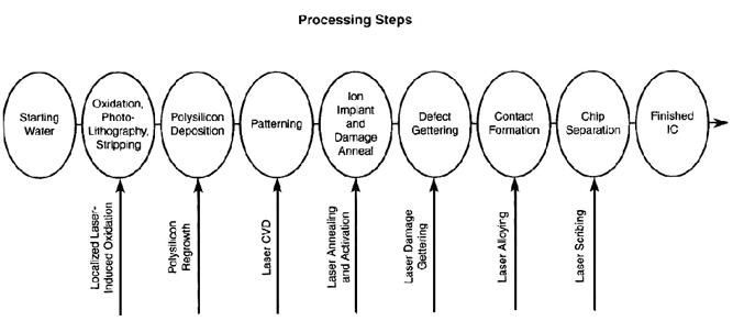
Another important research area in recent years has been the investigation of laser processing of semiconductor circuitry at the wafer level. This work, too, offers the possibility of extending the use of lasers to fabrication of the integrated circuit itself. The development of low-temperature processing technology is a key requirement. Laser radiation can provide fast localized heating that does not affect nearby portions of the circuitry. Figure 6. illustrates some of the possible steps where lasers can play a roll in the fabrication of semiconductor integrated circuits. The figure shows some representative processing steps common in the manufacture of semiconductor circuits but does not represent fabrication of any specific circuit. The figure also illustrates some of the ways in which laser processing could be applied to these steps.
Fig. 6 Typical processing steps for microcircuit fabrication and possible areas of laser impact
In the following discussion, we will emphasize two of these in detail: the annealing of ion implantation damage, and laser photodeposition of circuit patterns. The ideas for direct laser intervention in the fabrication of integrated circuits began with research into annealing of damage produced by ion implantation in semiconductor circuits. Ion implantation has become the preferred method for introducing impurity atoms into silicon to define circuit structures. The implantation performed with high-energy (perhaps 200 keV) ions damages the crystalline lattice of the silicon and makes it amorphous near the surface. Annealing is necessary to recrystallize the silicon. The annealing is conventionally done in a furnace. Laser annealing can also recrystallize the silicon and would have the advantage that the entire wafer is not heated. Laser annealing of ion implantation damage has been studied very extensively. It was found that laser annealing could regrow the crystalline structure, producing single-crystal silicon. Laser annealing removes defects, such as dislocation loops, which are common in furnace regrown silicon. It activates the implanted ions and thereby lowers the surface resistance. In addition, in contrast to furnace annealing, it can be done in such a way as to preserve the profile of the implanted ions. Laser annealing can be accomplished either by applying a very short (100 nsec) pulse of energy over an area of several square centimeters, or by scanning a continuous beam of small area over the surface of the material being processed. In the continuous case, the duration of processing for a particular area may be of the order 1 sec. This is much longer than in the pulsed case, but still short enough to retain the intrinsic advantages in comparison with conventional methods. Pulsed laser annealing of ion implanted layers has most often used Q-switched ruby or ND:YAG lasers with pulse duration around 100 nsec. Continuous wave laser annealing is performed with a beam from a continuous laser, most often an argon laser. The beam is scanned over the surface of the sample so as to provide continuous coverage. The laser power and scan speed are controlled to produce surface heating without melting. Thus, the process involves solid state regrowth, similar to the process that occurs in furnace annealing; for laser annealing, though, the heating is confined to a very thin surface layer, and the time scale is much shorter. Laser annealing of ion implantation damage with both the continuous method and the pulse method activates implanted ions and regrows the crystalline silicon well. In addition, the continuous laser annealing preserves the profile of the implanted ions.
Laser annealing of ion implantation damage in semiconductors was a popular research topic in the late 1970s and early 1980s. However, it has not yet become widely used in the microelectronic industry because of economic factors. Laser annealing of ion implantation damage has remained more expensive than furnace annealing.
Another potential application of laser technology in integrated circuit fabrication is the direct generation of patterns. For example, laser-aided chemical vapor deposition, which can be used to deposit layers of semiconductors, metals, and insulators, can define the circuit features. The deposits can have dimensions in the micrometer regime, and they can be produced in specific patterns. Laser chemical vapor deposition can employ two approaches: 1) A pyrolytic approach in which the heat delivered by the laser breaks chemical bonds in vapor phase reactants above the surface, allowing deposition of the reaction products only in the small heated area. 2) Direct photolytic breakup of a vapor phase reactant. This approach requires a laser with proper wavelength to initiate the photochemical reaction. Often, ultraviolet excimer lasers have been used. One example is the breakup of trimethyl aluminum gas with an ultraviolet laser to produce free aluminum, which deposits on the surface. Again, the deposition is only on the localized area that the beam strikes. A typical example might involve use of a krypton fluoride excimer laser operating at 249 nm with a pulse duration around 100 nsee and a pulse repetition rate that can be varied up to 200 Hz. For metal deposition, a fluence in the range from 0.1 to 1 joule per square centimeter per pulse is typical. The gas handling system is usually a dynamic flowing system, because the reactants in the gas chamber are constantly being replenished and by-products are removed. In contrast, in a static system, reactants are depleted and by-products build up. A variety of reactions have been investigated. One can deposit materials, including metals, insulators, and semiconductors. One can perform doping operations, etching, and stripping of insulating materials. All these operations can be done in a highly controllable fashion, depositing a material only on the areas where it is desired. Compared with conventional processing techniques, laser deposition allows fabrication of entire circuits all in a clean vacuum system without a need to move back and forth between different processing stages. Thus, it is a very clean technology capable of producing circuitry with very low levels of defects. The development of laser technology for direct generation of integrated circuits would provide an effective method of cool dry processing for microelectronics, useful in the preparation of solid state devices and their packaging.
Summary
The current status of laser applications in microelectronic fabrication is that laser technology has made substantial impacts on the fabrication of components such as the substrates and resistors. It is widely used for trimming both thick and thin film resistors, for scribing wafers, for hole drilling in substrates, for welding of hermetically sealed packages, and for stripping insulation from wires. The marking of silicon wafers with identification numbers has also become well established. In all these applications, lasers have become established production tools, replacing earlier technology for many applications. The applications of lasers in microelectronic fabrication have become accepted on a routine production basis because they offer economic advantages in many cases. Laser fabrication is an effective economic competitor for applications such as resistor trimming. In the areas of laser annealing and direct generation of patterns, the economic factors do not yet favor laser processing. At present, laser annealing of ion implantation is more expensive than furnace annealing. Hence, it has not been widely adopted except in a few specialized niche areas. It also faces strong competition from other regrowth techniques, including regrowth using strip heaters and arc lamps, These competing techniques have also yielded very favorable results. For the future, as feature sizes in integrated circuits continue to shrink, laser annealing may be needed to minimize the motion and diffusion of the implanted ions so as to reach the lowest possible values of feature size. Similarly, laser deposition of the integrated circuits on an entire wafer has been relatively slow and, hence, expensive. In addition, the process equipment used in the semiconductor industry represents a large investment that the manufacturers are reluctant to make obsolete. Therefore, laser direct write processing of integrated circuits has not reached production status. Near term applications will remain specialized; we may look for uses such as customization and personalization of integrated circuits. In these applications, selected pathways of metallization may be deposited or removed so as to change the operation of a specific circuit. Also, laser repair of expensive circuits is developing. One can replace missing metallization, for example, and hence salvage a high-value circuit that would be otherwise scrapped. For the longer term, we took toward advances in laser technology to provide high-power lasers that can be used with projection techniques to fabricate the entire circuit through a mask. This will increase the throughput and should remove existing restrictions on the time that it takes to fabricate an entire integrated circuit by direct write processing. With such advances, it is likely that laser deposition can become an effective economic competitor.
In conclusion, laser processing has provided many cost-effective solutions to probelms in microelectronic fabrication. We may expect these applications to burgoen in the future as laser processing plays more of a role in fabrication of the integrated circuit elements themselves.
For details of Basic Constructions of Lasers, please refer Level 1 chapter 2 section 2.4
![]()
![]()
![]()