|
Femtosecond/nanosecond
Laser-Induced Surface Texturing and Simultaneous Crystallization of
Hydrogenated Amorphous Silicon (a-Si:H)
Amorphous
silicon thin films have been considered for use in solar cell applications
because of their significantly reduced cost compared with bulk crystalline
silicon. However, their overall efficiency and stability are less than that
of their bulk crystalline counterparts.
This
project is to use both femtosecond and nanosecond (excimer) laser processes
of a-Si:H to solve the two disadvantages simultaneously. Both lasers
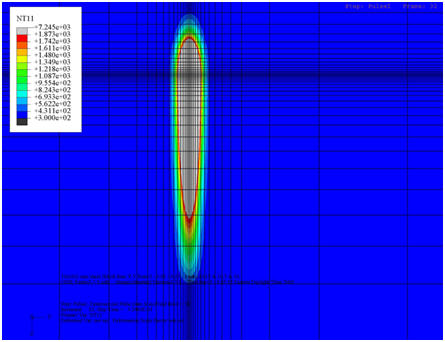
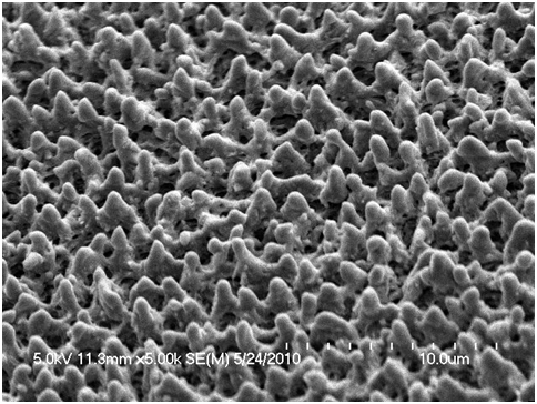
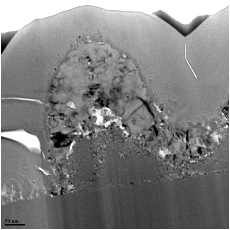
produces nano-/micro-meter size spikes which can be used for production of
periodic structures on the sample surface, and simultaneous crystallization
occurs in a one-step process. Optical absorption is enhanced by light
trapping via multiple reflections through the surface geometry changes, and
the formation of a mixture of crystalline silicon and a-Si:H after
crystallization suggests that the overall stability can be potentially
increased. Both laser-based treatments of a-Si:H show a promising
methodology for thin-film solar cell fabrication, and compared to
femtosecond laser, excimer nanosecond laser is more desirable for producing
large grains with low defects and preventing hydrogen from diffusing out
through a step-by-step process. |