![]()
![]()
![]()
Level 3
Section 5.3: Three Dimensional Micro-structuring in materials
Strategy:
Fabrication of true 3D microstructures is achieved by varying the exposure conditions. In one strategy, we can take the advantage of the varying bulk absorption of Futuran. A one-millimeter thick sample exposed to 355nm light would result in a latent image that is uniform through the thickness of the sample (assuming the incident fluence exceeds the minimum value for exposure.) On the contrary, if this sample were to be exposed to 248nm light the image will develop to only a depth where the critical fluence is maintained. Clearly, since exposed regions etch more rapidly than the surrounding areas, true 3D machining can be achieved by varying the photon flux and wavelength over different parts of the workpiece.
Another strategy to 3D rnicromachining involves illuminating the sample with a laser beam and shaping the beam. Structures with straight walls are obtained with a calumniated laser beam. Hyperboloids are formed with light that focuses or defocuses as the light passes through the material. One can also place the focus at the center of the material to create an hour-glass shaped latent image. Moving the workpiece in the XYZ direction during exposure increases the possible complexity of the produced part.
An interesting consequence of the unique processing of Foturan, is the texture of the resultant parts. Because the crystalline phase nucleates and grows into the glass and then is etched away, one can achieve widely varying morphologies. In figures 1 below, the remaining structures look as if material is scooped out of the side surfaces. In fact, the surface conforms to the growth of the crystal into the glass. Where grains intersect and etch away, the amorphous phase that remained in the interstices can possess very sharp edges, which we hope to exploit in field emission devices.
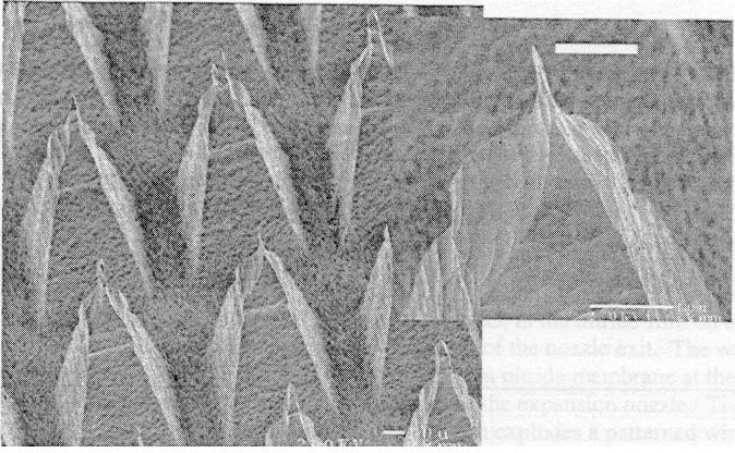
Figure 1: Etched Foturan microstructures. Note the tip's tight radius of curvature. (Peter Fuqua, et. al., 1999)
Applications
Thruster concepts
Cold Gas Thruster
The cold gas thruster is the most common. It typically consists of a pressurized gas chamber (propellant tank), a gas metering valve, a cavity chamber (gas plenum) and an hour-glass shaped exit nozzle. Cold gas thrusters usually possess low specific impulse and as a consequence great care is exercised in their design to insure the efficient conversion of the pressurized fuel to thrust. The miniaturization of the cold gas thruster poses significant challenges in maintaining efficiency. As fluidic devices are miniaturized, the surface area to volume ratio increases, which can result in larger drag, forces. The proper design of the exit nozzle is key to providing maximum thrust. A true 3D-axis symmetric hour-glass shape nozzle is more efficient than an extruded 2D hour glass nozzle. The use of photostructurable glass and laser direct-write processing permits the fabrication of 3D nozzles to a wide range of dimensions and an expansion ratios defined as the exit plane cross-sectional area is divided by the throat cross-sectional area. The processing variables include beam shape and position in the workpiece as well as laser fluence metering. It is important to choose a laser fluence that enables the exposure of the sample, but not initiate thermal effects within the volume of the beam. The Aerospace laser prototyping center was used to fabricate 3D axisymetric micronozzles in 1mm thick Foturan with a throat diameter of 100 microns and area expansion ratio of 10. Two nozzles, along with a laser fabricated gas plenum and commercial silicon MEMS valve (IC sensors), were assembled into a bi-directional 1mN class cold gas thruster. Figure 2 shows a picture of the thruster and figure 4 shows the thrust data. The largest measured specific impulse was 50% of the ideal specific impulse expected for argon with a 10: I expansion ratio. Without the MEMS valves, the thruster efficiency approached 80%. Comparison of the two configurations clearly shows that the gas flow is choked at the MEMS valve. This problem is mitigated by the use of a MEMS valve with a larger throat opening.
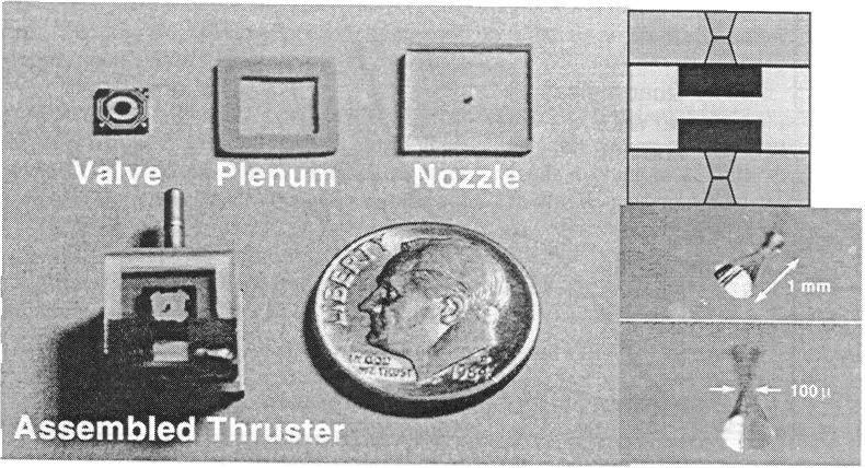
Figure 2: Cold gas thruster (Peter Fuqua, et. al., 1999)
Digital Thruster
Another Nanosat propulsion concept is that of the digital single-shot thruster. Here MEMS technologies could be used to create an array of miniature single use thrusters. One might imagine 10,000 single shot thrusters on a single wafer. Each thrust chamber would be independently addressable and each propellant chamber would be sealed. This approach mitigates the use of valves that add complexity and are prone to leakage. Satellite
Our embodiment of this concept involves 3 layers. The first layer is a silicon die with an array of heating elements or fuses, which ignite the fuel. The second layer is the propellant array chamber, fabricated from Foturan. The propellant cylinders are fabricated by direct-write patterning with the LTV laser and etched. The arrays of fuel cavities can be filled with any one of a number of fuels. The propellant chamber is capped with the third wafer layer. This layer contains an array of silicon expansion nozzles that are sealed at the throat by a silicon nitride diaphragm. The diaphragm array is produced from a silicon wafer coated on both sides with 5000A of silicon nitride. User ablation is used to create an array of breaches in the nitride film on one side of the wafer. The other side is left unpatterned. The breaches form the perimeter of the nozzle exit. The wafer is anisotropically etched in 35% KOH (60C) for a day leaving a silicon nitride membrane at the bottom of a truncated pyramidal pit. The square membrane forms the throat of the expansion nozzle. The fuel is ignited by delivering a pulse of electrical current to the heating element, which explodes a patterned wire. The pressure in the microchamber builds until the silicon nitride diaphragm bursts, producing a single pulse of thrust.
In figure 3 we show the three layers of the prototype thruster array. The first is the array of resistive polysilicon elements. The second figure is the Foturan propellant chamber. There are 15 chambers, each is 700 microns in diameter. The four smaller holes are for alignment with fiducials on the wafer below. Lastly is the array of laser patterned and KOH etched die.
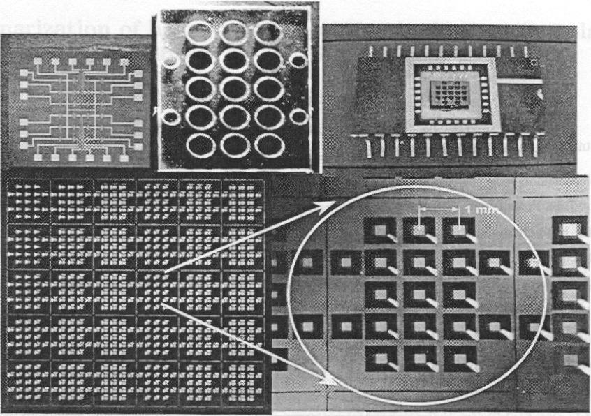
Figure 3: Digital thruster array. 1) Resistor wire igniter bottom wafer, 2) Laser fabricated propellant chambers typically 700 dia by 1mm deep. 3) Silicon nitride membranes (0. 15 microns) fabricated by laser ablation patterning and KOH bulk silicon etching. 4) Final package of the 3-wafer package wire bonded in a silicon- die chip holder package. (Peter Fuqua, et. al., 1999)
Figure 4 shows frames from high-speed videotape of a single cell ignition. In this experiment the 15 element array thruster is mounted on an IC flatpack chip and placed in a test fixture to measure thrust. The visual bum time is just over a 1 millisecond. Thrust measurements show that an average of 80 rnillinewtons is achieved for a propellant chamber 1mm long and 900 microns in diameter. The single ignition produces an equivalent power of 60 W.
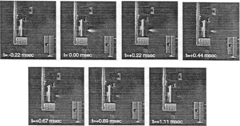
Figure 4: Video frames of solid propellant digital thruster firing on a thrust stand.
Average thrust is 80mN; equivalent power is 60W. (Peter Fuqua, et. al., 1999)
The use of direct-write laser processing for the fabrication of the digital thruster chip provides several advantages, given below.
- Rapidly prototype test chips with various chamber diameters.
- Individually alters the fuel chamber shapes and positions.
- Rework prior fuel chambers.
- Laser direct-write techniques can selectively seal individual chambers.
- Fabricate non-cylindrical chamber shapes and circular nitride membranes.
A direct-write laser micromachining volume exposure technique has been developed to fabricate true 3D microstructures in a photostructurable glass. This new technique, in conjunction with traditional direct-write ablation techniques, has been used to fabricate two types of rnicrothrusters for applications to l Kg class satellites. The results of the thrust measurements are promising and they open the door for fabricating microthrusters out of glass/ceramic materials that have certain advantages for space use. Laser based processing offers the rapid prototyping capability that is advantageous in the development of microthrusters, where the physics of fluids in microchannels is still an extraordinary science. Another advantage is that this processing is relatively clean with minimal debris for contamination.
Microelectronic technology
The integration of electronic mechanical and optical functions in single devices gets growing importance with the fast development of the Microsystems technology. There is a demand for such special devices with dimensions as small as possible. This trend is noticeable in a number of publications of the last time. Most of the devices for the Microsystems technology are produced with the well-known microelectronic silicon technology. The development of new devices requires however also the application of other materials e.g. glasses, ceramics and plastics, which couldn't or couldn't god processed with the microelectronic technology.
A obvious possibility to solve that problem is the application of lasers because of the chance to process nearly all materials. Therefore we have investigated the structuring of different materials by the excimer laser and TEA CO2 laser mask projection technique. Recently a considerable number of authors have reported on die use of lasers for micro material processing for instance of Si3N4 ceramics using excimer lasers as well as of ceramics and hard metal (Janson, 1994) and of glasses (Janson, 1995) using Nd:YAG lasers.
Exner, el. al., (1999) have been investigating the structuring of silicon, anodic bondable PYREX glass, A12O3-ceramic and PNIMA by means of laser microprocessing using an excimer laser (248 nm or 193 nm wavelength, 30 ns pulse duration, 400 mJ pulse energy) and a TEA CO2 laser (10,6 gm wavelength, 80 ns or 200 ns pulse duration, 6 J pulse energy). Both the mask projection technique and the focusing technique have been employed. They showed the dependence of the ablation thresholds and the ablation rates on the laser parameters and on the physical properties of the materials, i.e. absorption coefficient, melting point and thermal conductivity. During and after the laser processing of different glasses, they observed the formation of cracks in the laser-irradiated region and partly in the glass wafer surrounding the drilled holes. Those crack formations should be due to the development of thermally induced mechanical stress in the glass. They calculated the TEA CO2 laser ablation process using a half-empirical rotation symmetrical model.
They examined the feasibility of making various microscopic modifications in glasses by ultra-short pulses. It was confined that permanent refractive index changes, photo-reduction of samarium ions, the phenomenon of long-lasting phosphorescence, and creation of microcrystals with second-order nonlinear optical functions can be produced with a femtosecond pulse laser only in selective internal areas in glasses. By using a femtosecond laser with a high repetition rate, permanent optical waveguides can be successfully written in various glasses, where refractive index changes are continuously induced along a path traversed by focal point. We also confirmed that only rare earth ions of the core region in the waveguides are reduced by the laser irradiation.
Ultrashort-pulse laser machining of 3D GLASS structure:
The reactions between light and glass in photochromic, photosensitive and polychromatic glasses have been well researched. There has also been considerable research on the writing of Bragg gratings inside optical fibers and on photochemical hole burning. The reaction between light and glass has been put to practical use in phase-change-type memories using a heat-mode scheme. Such reactions are usually produced by exciting an absorption area on the glass to achieve various types of light-induced structural changes. Continuous-wave lasers and pulse lasers having pulse widths of nanosecond order and greater are used as light sources, and the laser wavelengths are mostly in the ultraviolet regions. As a consequence, light-induced reactions are more active on or near the surface layer of the glass; it is difficult to achieve light- induced effects only in selective internal areas of the glass.
In general, it is difficult to produce an interaction effect between glass and light by one photon process when the excitation wavelength does not agree with the wavelength of absorption region of the glass. However, various types of interactions with glass can be produced by using an ultrashort-pulse laser operating at the nonresonance wavelength with pulse widths of femtosecond order. Ultrashort light pulses are useful for observing and evaluating at a very high time resolution the dynamics of the phenomena that occur within materials at speeds ranging from pico- to femtosecond. Such phenomena include the direct interaction between light and atoms or molecules, the saturation process associated with the coherent state of materials, and the elementary process of chemical reactions. A short pulse width also means that extremely high peak power can be obtained and that high intensity light (up to1014 W/cm) can easily be achieved by focusing the laser. The development of high-energy-density femtosecond pulse lasers has prompted us to investigate the unexplored potential for inducing multiphoton photochemical reactions. There is therefore considerable interest in using femtosecond lasers to generate various types of microscopic, which are of scientific and practical interest.
K.Miura (1997) recently discovered that refractive index change of the order from 10-2 to 10-3 can be induced within various types of glass by irradiating the glass with focused femtosecond laser pulses."' By using a femtosecond laser with a high repetition rate, permanent optical waveguides can be successfully written in various glasses, where refractive index changes are continuously induced along a path traversed by focal point. They have also discovered the long lasting phosphorescence phenomenon, which can be observed with naked eye even 10 hours after the removal of the exiting.
More recently (K.Miura, 1999), it was confirmed that photo-reductions of rare earth ions in a few glasses could be produced by the irradiation of femtosecond laser pulses. Up to now, to our knowledge, no creation of permanent photo-redox reactions in the glass have been reported with the laser, although several investigations have been conducted on the transient creation of the divalent rare earth ions in solutions and halide crystals by laser irradiation. They described a variety of microscopic modifications which are permanent or metastable at room temperature can be made only in the laser focusing area inside transparent glasses by using femtosecond laser pulses. They also introduce the preparation and optical characterization of photo-written optical waveguides formed in bulk glasses by a ultrashort pulse laser in femtosecond region.
In general, it is difficult to produce an interaction between glass and a laser when the pulse energy is not absorbed by one photon absorption process. However, an ultrashort-pulse laser can produce various types of interactions with glasses through the nonlinear optical process. In practice, white-light generation due to the self-phase modulation and second-harmonic generation were observed from the focal point of the laser beam inside the glass.
With microscopic modifications in glass by the femtosecond laser, multiple photo-induced structures can be formed in the same area by the use of differences of thresholds for various types of photoreactions. For example, by making use the difference of thresholds for the refractive index change and for photo-reduction, it is possible to reduce only rare earth ions in the core area of the optical waveguide written by a femtosecond laser. Figure 5 shows an example of photo-reduction of samarium ions in a core area at an average laser power of 90 mW after writing an optical waveguide within samarium-doped glass with a 10X objectives and an average laser power of 200 mW. By the combination of photo-induced refractive index change and photo-reduction, it is possible to fabricate composite structure of microscopic modifications in which the emission and absorption characteristics of low refractive-index area and high refractive-index area are completely different. Composite formations of microscopic modifications by femtosecond laser pulses are an effective means of giving new functions to glass materials.
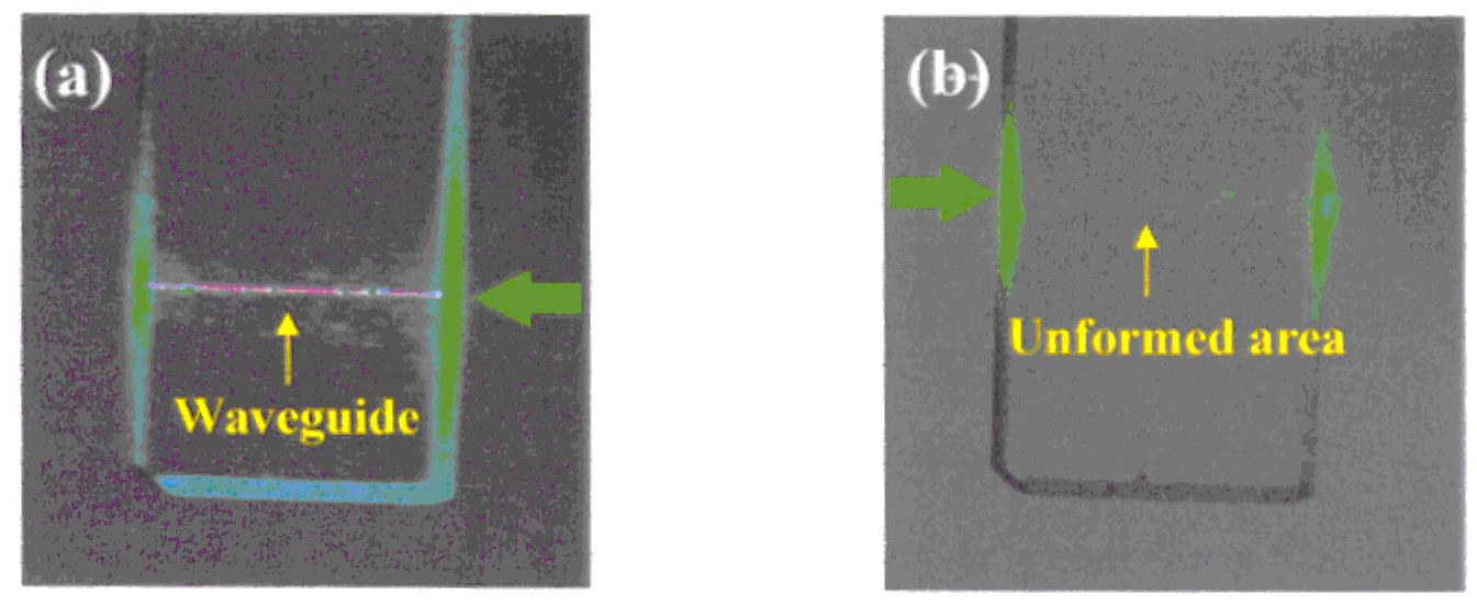
Figure 5. shows an example of photo-reduction of samarium ions in a core area at an average laser power of 90 mW after writing an optical waveguide within samarium-doped glass with a I OX objectives and an average laser power of 200 mW. (K. Miura, et. al, 1999)
In an attempt to form three-dimensional microscopic modifications in bulk glasses, Miura, et. al., (1999) have investigated various photo- induced structures produced by focusing an ultra-short laser pulse through a microscope objective. It was confirmed that permanent refractive index change, photo-reduction of samarium ions, long lasting phosphorescence phenomenon and precipitation of micro-crystals with excellent nonlinear optical functions can be produced only in selective internal areas with a femtosecond pulse laser. They investigated optical waveguides formed by using photo-induced refractive index change produced with an ultra-short pulse laser in the femtosecond region, and demonstrated that permanent optical waveguides could successfully be formed in various types of glass through our novel method. Because of the presence of a threshold for photosensitivity of each modification, it is possible to make microscopic modifications three-dimensionally in glasses by using a nonresonant femtosecond laser. In addition, it was confirmed that multiple photo-induced structures could be formed in the same area by the use of the difference of thresholds Our findings have opened up new possibilities in the production of novel functional optical materials and devices.
REFERENCES AN BIBLIOGRAPHY
S. W. Janson, Chemical and Electric Micropropulsion Concepts for Nanosatellites, Proceedings of the 30 th ALKA Joint Propulsion Conference, AIAA-94-2998 (1994)
S. W. Janson, Spacecraft as an Assembly of ASIMS, in Microengineering Technology for Space Systems, H. Heivajian Ed., Aerospace Technical Report ATR-95(8168)-2, 1995
Horst Exner, Bernd Keiper, Peter Meja, "Microstructuring of materials by pulsed laser focusing and projection technique ," Laserinstitut Mittelsachsen e.V., Hochschule Mittweida, University of Applied Sciences, Technikumplatz 17, 09648 Mittweida, Germany
Peter Fuqua, S.W.Janson, W.W.hansen, and H.Helvajian, 1999 "fabrication of true 3D microstructures in glass/ceramic materials by pulsed UV laser volumetric exposure techniques," Proc. SPIE 1999, p 213
K. Miura, J. Qiu, H. Inouye, T. N.fitsuyu and K. Ffirao, App. Phys. Lett. 71,3329,1997.
K. Miura, H. Inouye, J. Qiu, and K. Hirao, Nuclear Instruments and Methods in Physics Research B 141, 726, 1998.
K. Miura, H. Inouye, Y. Kondo, T. Nbtsuyu and K. Hirao, Appl. Phys. Lett. 73, 1763, 1998.
K. Miura, et. al, 1999, "Three dimensional microscopic modification in glasses by femtosecond laser", Proc. SPIE 1999, p141
![]()
![]()
![]()