![]()
![]()
![]()
Level 2
Section 5.6: Diode pumped laser machining of materials
Fundamenatals:
The basics of Diode Pumped Lasers is overviewed in level 3, sec 2.1. There are four types of pumping laser diodes, listed in order of increasing output power as: (1) single stripe; (2) diode array; (3) diode bar; (4) stacked bars. At the lower end of the output power range (P < 100 mW) is the single-stripe semiconductor laser. By means of a suitable insulating oxide layer, the diode current is confined to a 3-5m m wide stripe extending over the entire length of the diode. The emitted beam has an elliptical shape with a diameter in the direction perpendicular to the laser junction of ~lm m and a diameter in the junction plane of 3-6m m. With such small spot sizes, the beam is spatially coherent, i.e., it is diffraction-limited. Note that, in view of this strong difference between beam divergences in the two directions, the beam's major axis direction is rotated by 90 degree after beam propagation just a few micrometers away from the diode exit face.
To obtain greater output powers, one uses a monolithic array of diode-laser stripes, fabricated on the same semiconductor substrate. In typical cases, the array may contain 20 stripes, each 5 m m wide, with their centers spaced by ~10m m. Actually, for lower power devices, some phase correlation among various emitters may develop, leading to a characteristic two-lobed angular emission pattern, with the two lobes spaced by - 10o and each - 1o wide. Output power from such arrays may be up to ~ 2 W.
To obtain still greater output powers, the previously described array can be serially repeated in a single substrate to form a monolithic bar structure. It consists of 20 arrays whose centers are spaced by 500m m; each array is 100 m m long and contains 10 laser stripes. The overall length of the bar is thus 1cm, the limit being set by processing technology. Again all stripe emitters can be considered phase uncorrelated and output powers up to 10-20W are usual.
The bar concept can be extended to the case of a stack of bars forming a two- dimensional structure. Six 1-cm-long bars are stacked to form an overall 2mm x 1cm emitting area. These stacked bars are intended for quasi-cw operation with a duty cycle up to 2%. (Peak power density may be up to 1kw/cm2and average power up to 100 W/cm2.)
To pump laser materials, such as ND:YAG, having narrow absorption lines, the width of the diode's spectral emission must be considered. The spectral emission bandwidth of a single stripe may be as narrow as I nm, which compares favorably with, e.g., the ~2 nm bandwidth of the 808-nm absorption peak of ND:YAG. For the case of arrays and even more so, for bars or stacked bars, spectral emission can be substantially greater than this value due to compositional variation between stripes and due to temperature gradients, both of which leading to different stripe-emission wavelengths. Currently, the best results for a bar may be a spectral width as low as ~2 nm. To tune and stabilize the emission wavelength, diode lasers are normally cooled by a thermoelectric cooler, for low power devices, and by liquid cooling for the highest powers.
Applications:
The laser is an unstable resonator with a graded reflectivity outcoupler, generating a beam with excellent beam quality. The gain medium is a single zig-zag slab, pumped symmetrically by diode arrays. The use of diode arrays minimizes the thermal loading on the slab, and the zig-zag path averages thermal distortions in the zig-zag dimension. To date, the laser has produced 720 W at 20% diode duty-cycle with a stable cavity and 550 W at 20% duty cycle with an unstable cavity.
For example, drilling by laser radiation with minimal hole diameters in the range of a few 100 pm is state of the art. Holes with diameters smaller than 100 mm are of interest for e.g. power engineering, automotive and aircraft industry.
For these applications high beam quality, small heat effected zones possibly with recast layer and high reproducibility are necessary. Nanosecond and picosecond laser radiation offers new possibilities by achieving higher accuracy. Because of the short pulse lengths higher power densities can be reached and rapid heating can lead to an earlier evaporation of the material and to a reduced recast which resoldifies after the end of the laser pulse at the boundaries of the holes. Therefore, a diode pumped picosecond laser system is developed to achieve high-energy pulses with short pulse length. Picosecond laser pulses are a promising tool for the production of microstructures and ultraprecise removal of thin layers.
For ultrashort laser pulses in the picosecond and femtosecond regime the deposition of optical energy in the material is different from the physical conditions during material processing of nano- and micro-second laser pulses. The finite time needed to convert optical energy of the material to internal energy by the electrons of the lattic must be considered. Therefore, ultrafast laser heating of metals must be described by three processes: the deposition of optical energy in electron-gas, the transport of energy by electrons and the heating of the lattice through electron-phonon interaction.
Ceramics:
The removal rate per pulse of Si3N4 ranges from 0.05m m to 0.25 m m in the investigated regime of 3.3 * 109 W/cm2 to 1* 1011 W/cm2. Because of measuring lower removal rates by l =355nm than by l =1064 nm and higher values by l = 532 nm, there seems to be no depending on wavelength perceptible. The removal rate per pulse of SiC seems to depend on the wavelength in the investigated regime. The removal rates are increasing with decreasing wavelength (Fig.3).
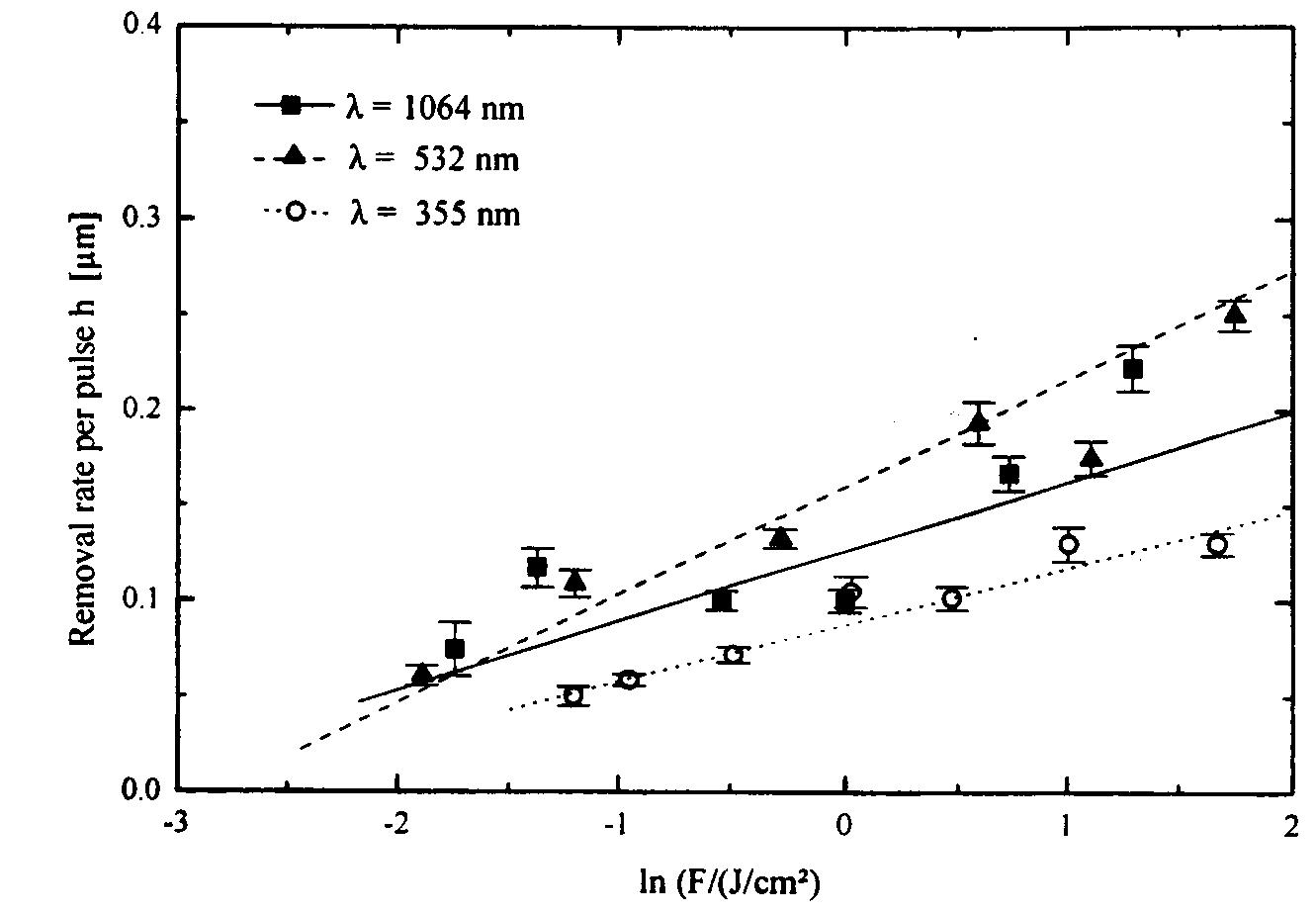
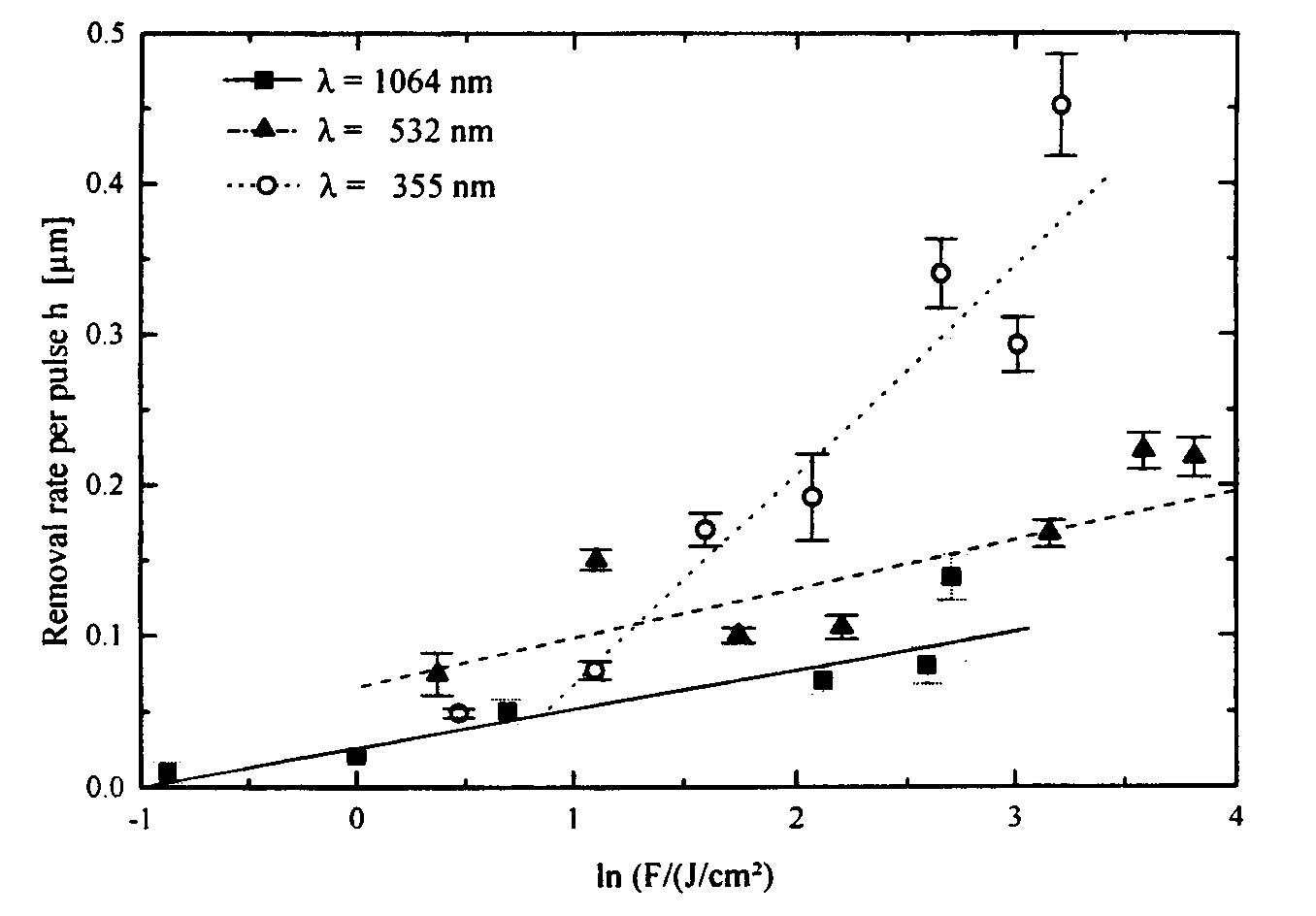
Fig 3. Removal rate per pulse of Si3N4 (left) and SiC (right) (R.Weichenhain, et al., 1999)
Polymers: The removal threshold and the removal rate per pulse were investigated (R.Weichenhain, et al., 1999) for the wavelength l =355 nm and the pulse length tp =30 ps. The removal rate per pulse of polyimid ranges from 0.01m m to 0.25 m m in the investigated regime of 7*107 W/cm2 to 6*109 W/cm2 and is in the same order of magnitude as by l = 24 8 nm and tp = 10ns.
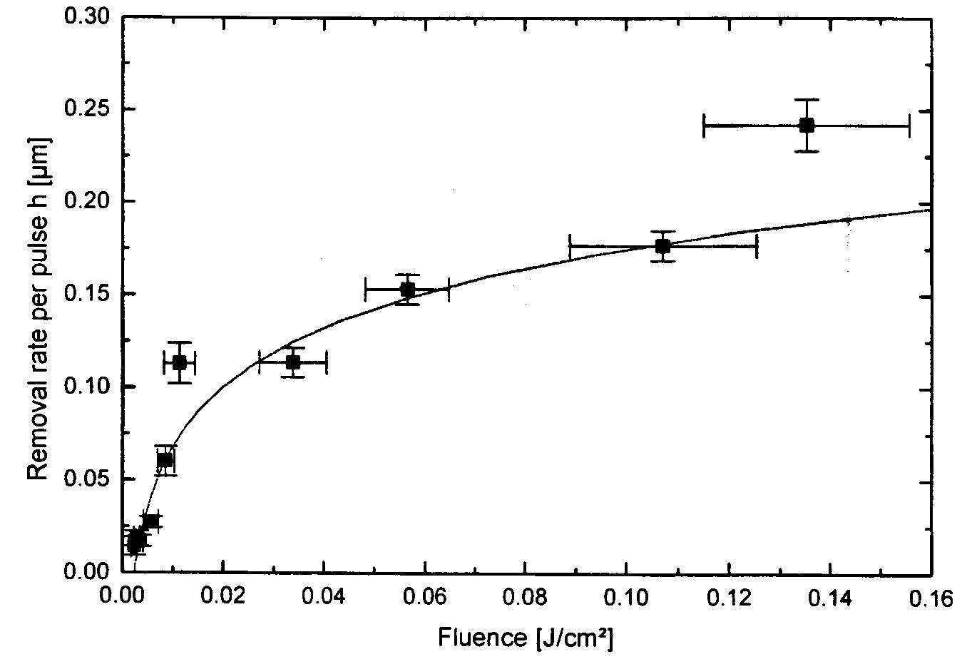
Fig 4. Removal rate per pulse of polyimid, l =355nm, tp=30ps (R.Weichenhain, et al., 1999)
Holes were produced in Si3N4, SiC and Polyimid using the second harmonic wavelength of l = 532 nm. In spite of different magnification a smaller heat affected zone in Si3N4 in case of the lower intensity (Fig.5a and b) is perceptible. The structure in SiC is marked by sharp edges (Fig 5 c).
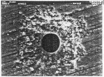
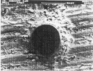
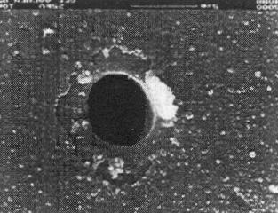
Fig 5. a) SEM images of holes in ceramics, tp =35ps, l =532nm, a) Si3N4, I=2.4*1012W/cm2, rf=6m m, d=20m m, b) Si3N4, I=1.1*1012W/cm2, rf=4.8m m, d=13.4m m c) SiC, I=1.2*1011W/cm2, rf=3.1m m, d=5m m (R.Weichenhain, et. al., 1997)
The recondensated particles in the surrounding of the hole could easily removed by chemical or mechanical means. The drillings in Polyimid are through holes. On the frontside the hole diameter is 7.5m m and the edges are characterized by continuous tapering from the surface into the hole (Fig.6 c). On the backside the hole diameter amounts to 2.5 vm with molten rims at the edge of the holes.
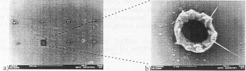
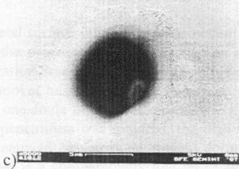
Fig 6. a) SEM images of holes in polyimid, tp =35ps, l =355nm, I=2.4*1012W/cm2, rf=7.5m m, d=20m m, b) backside: d=2.5m m, c) frontside: d=7.5m m (R.Weichenhain, et. al., 1997).
While developments in the field of diode pumped solid state lasers provide a foundation for precision machining of parts with high accuracy and small feature sizes, this promise can not be realized without considering the interactions of individual processes, systems and material parameters. Nikumb, Suwas K.and Islam, Mahmud U.(1999) presented the precision machining of small features in various materials using diode pumped solid state lasers. The machined features were characterized geometrically by using optical inspection techniques. Machining parameters relevant to motion system and tool path compensation were discussed along with their relevance to machined feature geometry. The effect of laser beam polarization on the machined kerf width, kerf surface and feature dimensions is reported.
Ceramics like Si3N4, Al2O3 (sapphire) and ZrO2 and also diamonds can be hardly machined by conventional methods. Short pulse lasers, especially frequency-tripled, diode pumped Nd:YAG-lasers with a high beam quality offer the possibility to ablate these materials with high quality (Hellrung, Dirk, et. al., 1999). With a spot size of about 10 µm, high fluences (> 100 J/cm2) can be achieved, so that the materials are vaporised without or with only a small amount of molten material. This technique is applicable for drilling small holes with diameters greater than or equal 5 µm (aspect ratio up to 60) and cutting of thin ceramic substrates (thickness < 0.5 mm). The edges are sharp and the face of the cut is very smooth. Furthermore it is possible to ablate three dimensional microstructures. Therefore the laser beam is scanned over the surface and the material is ablated pulse beside pulse. The surface roughness depends on the overlap of the laser pulses, the pulse energy and the scanning strategies. With optimised machining parameters the surface roughness can be reduced to Ra less than or equal 0.1 µm. Due to the low ablation rate of around 0.05 µg/pulse the ablation depth of a single slice can be controlled very precisely. Depending on the material and the machining parameters the depth is in the range of 1 to 10 µm.
Diode pumped solid state lasers with high beam quality improve the quality of laser beam removed micro-structures and opens the possibility to use this technology as a new manufacturing method for producing micro-tools. Predestined materials for the 3-dimensional micro-structuring by laser beam removal are hard materials such as ceramics and hard metals. These tools can be used to form processes of metal parts, like stamping, embossing or cutting (Hellrung, D., 1998).
![]()
![]()
![]()