![]()
![]()
![]()
Level 2
Section 5.4: Laser machining by doubled and tripled frequency YAG lasers
Ceramics:
For example, for the fundamental wavelength of the Nd:YAG laser the absorption of many ceramics is poor,. Using higher intensities, the disadvantage can be compensated and melting, vaporization and removal of material is also possible. But the process efficiency and often then machining quality is low. Furthermore the smallest structure size are restricted. Therefore, frequency-tripled Q-switch Nd:YAG lasers as well as Excimer-lasers can improve the process because the absorption is higher in the UV-range. Machining parameters and results have been investigated for ZrO2, A12O3, Si3N4, Diamond and WC (Dirk Hellrung, el. al., 1999)
The laser source is a Q-Switch diode pumped solid state laser (DPSSL) with an extra cavity frequency doubling and tripling (R. Koch, 1999). The beam profile can be approximated as a gaussian mode, which results in a near-diffraction limited beam. The laser beam has a high energy stability, which is important for the machining quality. The pulse repetition rate is in the range of 1 to 5 kHz. With different beam guiding and shaping devices the focus diameter can be varied between 3 and 20 m m.
The laser is combined with a 4-axis positioning system where the optic is fixed on the z-axis. The x-y-q -axis moves the workpiece underneath the focused laser beam. In most cases the laser beam is focused on the surface of the workpiece. The linear drives provide a high dynamic behavior with a maximum velocity of 500 mm/s. Due to the resolution of 0.1 m m a positioning accuracy of I gm can be achieved. The axis motion is controlled by a CNC-interface. Because the laser pulses cannot be triggered on demand but are fixed at a chosen pulse repetition rate, a special logical device synchronizes the laser pulses with the velocity of the axis to avoid grooves at the edges due to the acceleration and deceleration.
A CCD-camera is integrated to observe the process. The machined structures can be directly measured with a white light sensor (CHR 150 N). This sensor uses the chromatic aberration of a lens and has a measuring range of 300 gm at a resolution of 1gm and a spot size of 1gm. The lateral dimensions of the area are only restricted by the maximum way of the positioning tables and with adapted strategies also a larger z-range can be measured. With this sensor single point measurements, line and three-dimensional scans can be recorded and the corresponding roughness R,, will be calculate. The white light sensor is also used in an off-line control loop for the three dimensional laser beam removal process. Additional measurements are done with an optical and a scanning electron microscope (SEM).
MACHINING WITH SINGLE LASER PULSES
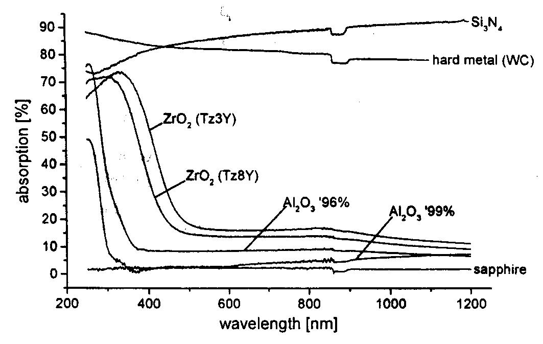
Figure 1 shows the absorption versus the wavelength in the interesting spectrum from 200 to 1200 nm. The values for the absorption are calculated from the measured reflection and transmission. The measurements are done only at low energies with a white light lamp, so that they cannot give an exact value for the laser process but they figure out the general course. The absorption increases rapidly in the UV-range for A12O3 and ZrO2. For Si3N4 and hard metal (WC) there is no significant change over the whole spectrum as well as sapphire is nearly transparent. But at high intensities or with a rough surface also sapphire can be machined.
Figure 1: Absorption of different hard materials
The effective working diameter does not need to be equal to the focus diameter but depends directly on the maximum power of the beam profile and the material specific threshold. So the effective diameter can be adjusted by the laser power and the beam shaping. Different investigations on threshold fluences of ceramics show that the values are in the range of 0.2 up to 1.5 J/cm2 which is very low compared to the maximum possible fluences of the used laser source. But for the reduction of the surface roughness, the minimization of debris around the machined area and the accuracy of the structure, which are important for the three-dimensional rnicrostructuring and the drilling and cutting, it is necessary to reduce the energy density. This is done by an external reducer, which can vary the laser beam energy from 0 to100 %.
Vice versa higher energy densities, which can be achieved by increasing the laser beam energy or decreasing the focus diameter, produce a deeper mould at a single laser pulse. Because of that the machining time will be reduced, but it causes more molten and damaged material. Therefore the energy density has to be adapted for different applications.
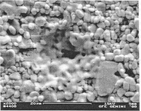
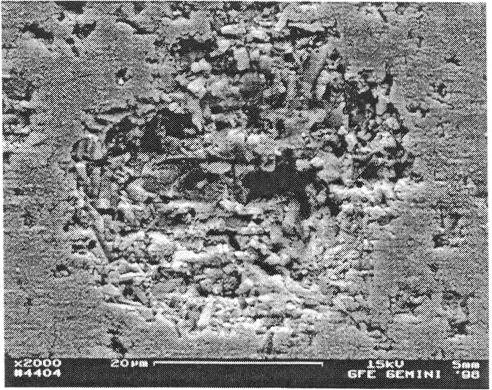
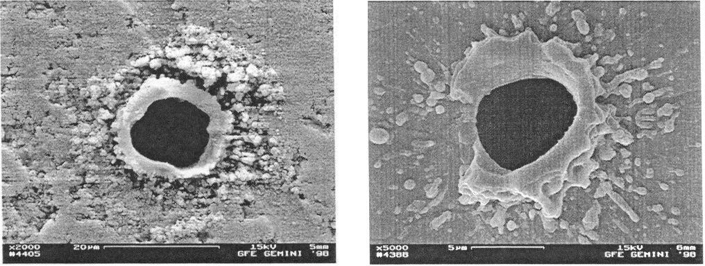
Figure 2: Single laser pulse moulds on A1203 and Si3N4 (k= 355 nm, fp= 1kHz, Ep= 0.56 mJ) (D. Hellrung, et. al., 1999)
Figure 2 shows the mould of different ceramic materials. The amount of molten material varies between different materials and can be reduced to a minimum. The grain sizes also influences the quality of the machined ceramic. During the removal process not only vaporization of material takes place, but also the removal of whole grains, due to the high pressure of the vaporized material. Single grains can be detected in the surrounding area of the moulds.
Drilling and cutting
The drilling process has been investigated for different ceramic materials (Dirk Hellrung, el. al., 1999). The thickness for all ceramics was 0.25 mm so that a single pulse drilling was not possible. For small holes the percussion drilling was used. Comparable to results for drilling of metals with a pulsed Nd:YAG-laser the diameter of the holes is dependent of the irradiation time. After a laser parameter and material specific time, which is necessary for drilling through the given material thickness, the hole diameter increases. But at longer irradiation times a pulsation of the hole diameter can be observed. The hole opens and closes again, until it reaches a final diameter. This is caused by the production of molten material on the edges of the hole, where the energy density is not high enough, to vaporize the material. The molten material flows to the center of the hole and s removed out of the hole with the following laser pulses. So the hole diameter depends on the irradiation time. This Pulsation is independent on the total energy density at the working position.
But the energy density at the focal position influences the maximum diameter, the removal depth per pulse respectively the time for drilling through the material and the maximum depth of a hole. The energy density can be easily varied by the pulse repetition rate. At higher pulse repetition rates the pulse energy decreases.
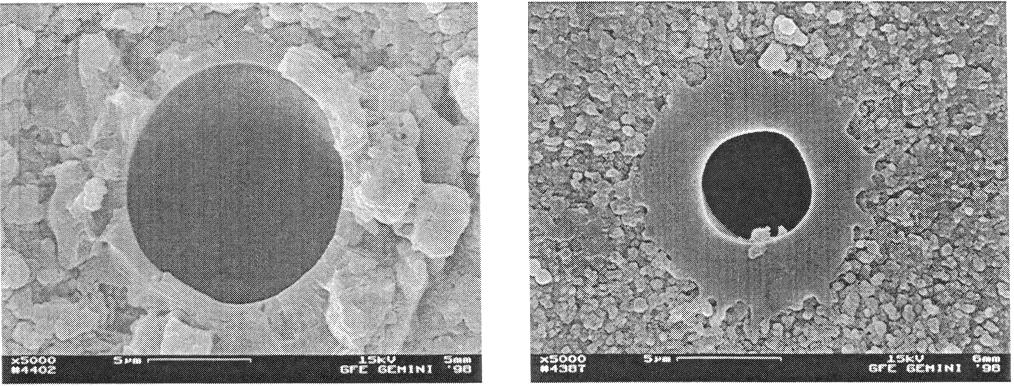
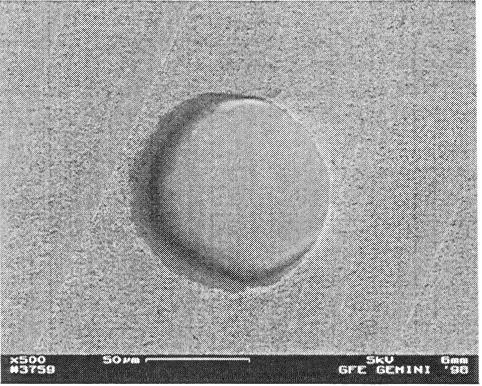
Similar to the ablation or removal process of an Excirner-laser, the removal depth per pulse has a maximum value at a material specific energy density. After that the amount of removed material decreases. But the best results are achieved at lower intensities, because higher intensities causes a damage of the surrounding material. In the range of investigation a damage of the edges caused by removed grains could only be observed at high energy densities. Furthermore the thickness of the recast layer could be reduced down to < 5 m m. Typical holes for A12O3, ZrO2 and diamond are shown in Fig. 5 and Fig. 6. The material properties of the recast layer, e.g. the hardness and the existence of micro cracks, have not been investigated due to the small size of the holes. It is possible that due to the thermal shock behavior of ceramics a small layer of damaged material could exist under the recast layer. Investigations with shorter pulse length show no significant advantage [9]. At higher energy densities also laser pulses in the fs-range can cause a material damage. So the machining quality is dependent on the maximum pressure of the vaporized material. The pulse length influences only the amount of molten material.
Fig. 5: Hole in A1203 (thickness 250 gm): entrance (left) exit (right) (l = 355nm, fp= 5 kHz, Ep= 0.22 mJ) (D. Hellrung, et. al., 1999)
Fig. 6. Hole in ZrO2 (thickness 250 gm): entrance (left) exit (right) (k= 355nm, fp= 5 kHz, Ep= 0.23mJ) (D. Hellrung, et. al., 1999)
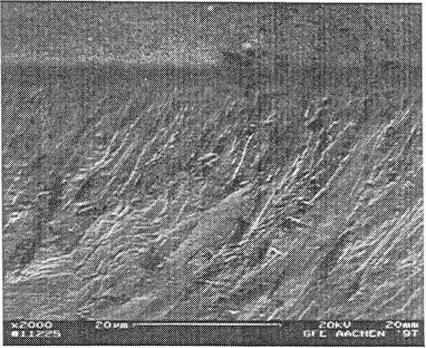
To produce larger diameters the holes have to be trepanned. Therefore the laser beam is guided over the workpiece several times along the cutting line. Fig. 7 shows the cut edges of Si3N4 and diamond. The cut edges are very smooth. For both materials no molten material can be detected. The cutting speed is about 100 m m/s.
Fig.7: cutting edge of (l = 355nm, fp= 5 kHz, Ep= 0.34 mJ) and polycrystalline diamond (l = 355nm, fp= 5 kHz, Ep= 0.34 mJ) (D. Hellrung, et. al., 1999)
3D-Microstructuring
To produce 3-dimensional microstructures with a direct writing laser beam removal process a relative movement between the laser beam and the workpiece is necessary, which is realized in most cases by straight lines. Several lines side by side produce a removed layer. For a 3-dimensional microstructure the geometry is sliced into several layers comparable to a milling process. This can be done by a CAD/CAM-software. The average depth of a single layer is a needed parameter for the calculation of the toolpath. After removing each layer, the exact depth of the layer is measured with the white light sensor and compared with the desired value. Any deviation can be adjusted by varying the process parameters or recalculating the toolpath. In this way very precise microstructures are produced.
At an overlap of 30-50 % a good surface roughness can be achieved. Out of this range the roughness increases steep. Furthermore the energy density influences the depth of a single layer and the roughness. The surface roughness increases at higher aspect ratios of a single pulse mould (removal depth of a single laser pulse in comparison to the effective working diameter). A periodic wavy surface is the result, where the period of these waves is not a function of the grid of the laser pulses. Figure 9 shows the surface of ZrO2, where the spatial distance between two laser pulses was 10 m m and the period of the waves is around 40 gm.
An optimized surface roughness can be achieved with flat removed areas, that means a low aspect ratio of the single pulse mould (see Fig. --). Especially the pyramid made Of Si3N4 has a very good surface roughness, which is in the range of the raw material. The height of the steps is around 100 m m. The quality of the edges is very good. Due to the low energy densities damage caused by removed grains could not be detected. The debris is very low and the removed material has only a very weak adhesion to the basic material, so that the structures can be cleaned in an ultrasonic bath.
Fig.10: Surface of A17,03 (X= 355nm, f,= 5 kHz, Ep= 0.3mJ) and Si3N4 (k= 355nm, fp= 5 kHz, Ep= 0.26mJ) (D. Hellrung, et. al., 1999)
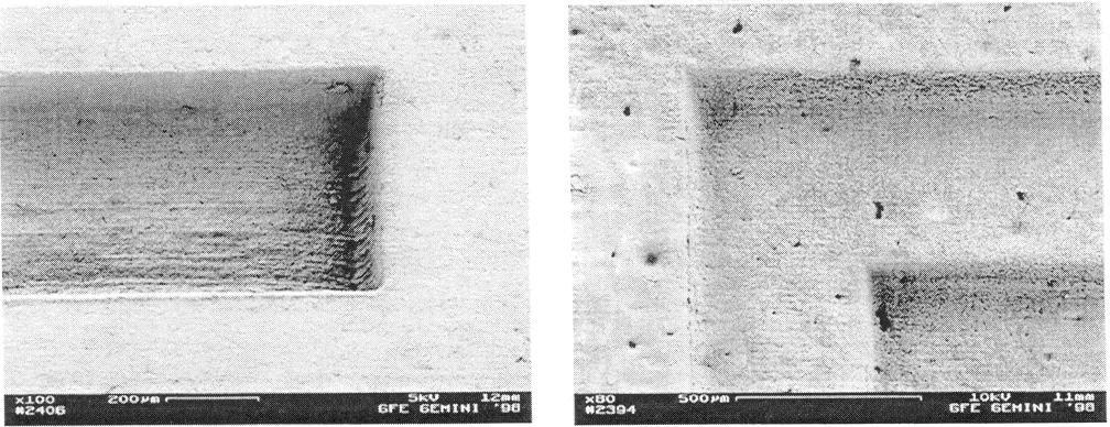
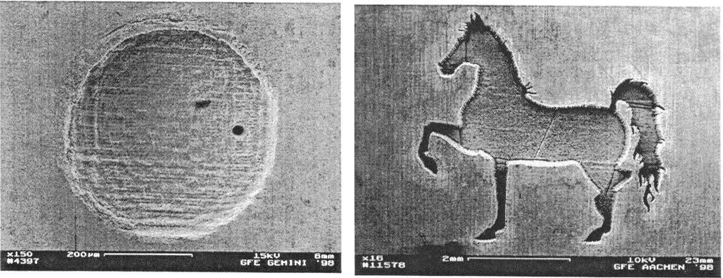
Compared to the combined mask and direct writing process with an Excimer-Laser, the direct writing process with a Q-Switch Nd:YAG-laser offers a higher flexibility concerning the possible shapes [101, because curved lines can be generated by the CAD/CAD-system (Fig. 11). The main restrictions are caused by the accuracy of the moving system. With this technique real three-dimensional structures can be produced. The final structures can be used as tools for the production of embossed metal micro parts.
Figure 11: Structured hard metal (WC) (k= 355nm, fp= 5 kHz, Ep= 0.34m3; depth = 0.1 mm resp. 1.5 mm) (D. Hellrung, et. al., 1999)
Polymers
Many materials are best machined using UV lasers sources which until recently has been the principal laser used in UV machining applications. The UV outputs available from frequency doubling of CVLs can now be generated with good efficiency to yield multi-watt diffraction-limited output ideal for UV micromachining. Recent progress has come through a greater understanding of the control of CVL beam quality and improvements in focusing geometries for the nonlinear frequency conversion process.
Glover (1995) reported high-speed ultra-violet (UV) micromachining of polymers using a high beam quality frequency-doubled copper vapor laser (CVL). The characteristics of the UV laser source and beam delivery optics are described. Measurements of material removal rates have been made for a number of polymers. Results for UV-CVL micro-drilling of PETG and polyamide (kapton) show removal rates per pulse similar to other UV sources, but the high pulse repetition frequency of the UV-CVL results in much enhanced temporal material removal rates.
Illy, Elizabeth K et. al., (1999) have previously shown that the material removal rate scales linearly with pulse rate up to 15 kHz for pulsed UV-laser ablation of polymers, giving the potential for substantial gains in processing speeds in ablative micromachining using high-pulse-rate UV sources such as frequency-doubled copper vapour lasers and frequency-quadrupled diode-pumped solid-state lasers. These rapid processing speeds can be effectively utilized in direct-write UV-laser micromachining including trepanning. In this paper we present studies of machining rates for trepanning of a strongly absorbing polymer (PETG), and a weakly absorbing polymer (PMMA), aimed at establishing optimum conditions of pulse rate, linear write speed (laser spot overlap) and laser fluence for maximum machining rates and high quality of the machined structure using a high-pulse-rate (5kHz) UV-CVL. For fixed fluence and pulse rate, machining rates for PETG are found to be independent of write speed in trepanning, however for PMMA machining rates increase for decreasing write speed (increasing laser spot overlap) where cumulative heating leads to enhanced dynamic etch rates. In the latter case, while reduced machining times can be achieved for high spot overlaps, this is generally at the expense of significant degradation in finish quality of the machined structure
Facrifation of optical fiber
Precision openings for construction of an optical backplane have been machined in an optical fiber using an excimer laser operating at a wavelength of 193 nm. The openings were made by imaging the laser beam onto the polymer fiber cladding with a telescope, then ablating the cladding with a sufficient number of pulses to expose the core. Circular openings measuring 250, 625 microns and elliptical openings measuring 650 × 350 microns have been made in the cladding of a 1 mm polymer-clad silica fiber. Examination by scanning electron microscopy reveals that the best quality openings are obtained with either the smaller circular geometry or the elliptical geometry. For various reasons, elliptical openings, with the major axis oriented along the longitudinal axis of the fiber, appear more suitable for tap construction. Individual optical fiber taps have been constructed by attaching a tap fiber to a laser machined opening in a central fiber using a ultraviolet-curable acralate. Individual tap measurements were made on the elliptical and the 250 micron circular openings. In addition, a triple tap assembly was made using elliptical tap openings. These results indicate that the excimer laser machining technique may be applicable to the
Rapid prototyping of micromechanical devices
A laser technology for fabricating microelectromechanical components has been developed. Using a Q-switched Nd:YAG laser with optional frequency doubling, bulk silicon wafers and silicon membranes are micromachined without lithography-based technologies. The shape and depth of the cutting kerf is influenced by the position of the focal plane. Laser cutting of silicon reduces the breaking limit of the silicon structures. Using a cleaning process in HF and KOH, the breaking limit can be brought back to its original value. Direct laser writing without has structured gold thin films deposited on silicon damaging the substrate. Using silicon and thin-film laser machining, rapid prototyping and small lot production of microelectromechanical devices (MEMS) has been realized.
![]()
![]()
![]()